(China (Mainland))


Product Summary
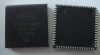
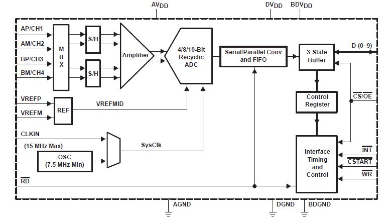
The TLV1562IDW is a 10-bit CMOS low-power, high-speed programmable resolution analog-to-digital converter based on a low-power recyclic architecture. The unique architecture delivers a throughput up to 2 MSPS (million samples per second) at 10-bit resolution. The programmable resolution allows a higher conversion throughput as a tradeoff of lower resolution. A high speed 3-state parallel port directly interfaces to a digital signal processor (DSP) or microprocessor (mP) system data bus. D0 through D9 are the digital output terminals with D0 being the least significant bit (LSB). The applications of the TLV1562IDW include Portable Digital Radios, Personal Communication Assistants, Cellular, Pager, Scanner, Digitizers, Process Controls, Motor Control, Remote Sensing, Automotive, Servo Controls, Cameras.
Parametrics
TLV1562IDW absolute maximum ratings: (1)Supply voltage range: AVDD (see Note 1): -0.5 V to 6.5 V; (2)BDVDD, DVDD (see Note 2): -0.5 V to 6.5 V; (3)AVDD to DVDD or BDVDD: -6.5 V to 6.5 V; (4)Voltage range between AGND and DGND or BDGND: -0.3 V to 0.5 V; (5)Digital input voltage range, CLKIN, CS, WR, RD, CSTART (see Note 2): -0.3 V to DVDD +0.3 V; (6)Digital data input voltage range: -0.3 V to DVDD +0.3 V; (7)Digital data output voltage range: -0.3 V to DVDD +0.3 V; (8)Analog output voltage range, INT: -0.1 V to AVDD+ 0.1 V; (9)Reference input voltage range, REFP: -0.1 V to AVDD+ 0.1 V; (10)Reference input voltage range, REFM: -0.3 V to 0.3 V; (11)Peak input current (any input): 20 mA; (12)Peak total input current (all inputs): -30 mA; (13)Operating free-air temperature range, TA: -40℃ to 85℃; (14)Storage temperature range: -65℃ to 150℃; (15)Lead temperature 1,6 mm (1/16 inch) from the case for 10 seconds: 260℃.
Features
TLV1562IDW features: (1)2 MSPS Max Throughput at 10 Bit (Single Channel), ±1 LSB DNL, ±1 LSB INL MAX; (2)3 MSPS Max Throughput at 8 Bit (Single Channel), ±1 LSB DNL, ±1 LSB INL MAX; (3)7 MSPS Max Throughput at 4 Bit (Single Channel), ±0.4 LSB DNL, ±0.4 LSB INL MAX; (4)No Missing Code for External Clock Up to 15 MHz at 5.5 V, 12 MHz at 2.7 V; (5)ENOB 9.4 Bit, SINAD 57.8 dB, SFDR–70.8 dB, THD –68.8 dB, at fi = 800 kHz, 10 Bit; (6)Wide Input Bandwidth for Undersampling (75 MHz at 1 dB, >120 MHz at –3 dB) at Rs = 1 kW; (7)Software Programmable Power Down, (1 mA), Auto Powerdown (120 mA); (8)Single Wide Range Supply 2.7 VDC to 5.5 VDC; (9)Low Supply Current 11 mA at 5.5 V, 10 MHz; 7 mA at 2.7 V, 8 MHz Operating; (10)Simultaneous Sample and Hold: Dual Sample and Hold Matched Channels Multi Chip Simultaneous Sample and Hold Capable; (11)Programmable Conversion Modes: Interrupt-Driven for Shorter Latency Continuous Modes Optimized for MIPS Sensitive DSP Solutions; (12)Built-In Internal/System Mid-Scale Error Calibration; (13)Built-In Mux With 2 Differential or 4 Single-Ended Input Channels; (14)Low Input Capacitance (10 pF Max Fixed, 1 pF Max Switching); (15)DSP/m P-Compatible Parallel Interface.
Diagrams
| Image | Part No | Mfg | Description |  |
Pricing (USD) |
Quantity | ||||||||||||
|---|---|---|---|---|---|---|---|---|---|---|---|---|---|---|---|---|---|---|
 |
 TLV1562IDW |
Texas Instruments |
ADC (A/D Converters) 10bit Programmable |
Data Sheet |
|
|
||||||||||||
|
TLV1562IDWG4 |
Texas Instruments |
ADC (A/D Converters) 10-Bit 2 MSPS Quad Channel |
Data Sheet |
|
|
||||||||||||
|
TLV1562IDWR |
Texas Instruments |
ADC (A/D Converters) 10-Bit 2 MSPS Quad Channel |
Data Sheet |
Negotiable |
|
||||||||||||
|
TLV1562IDWRG4 |
Texas Instruments |
ADC (A/D Converters) 10-Bit 2 MSPS Quad Channel |
Data Sheet |
Negotiable |
|
||||||||||||