(China (Mainland))


Product Summary
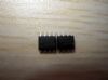
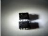
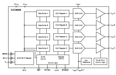
The DAC8565IAPW is a low-power, voltage-output, four-channel, 16-bit digital-to-analog converter (DAC). The device includes a 2.5V, 2ppm/℃ internal reference (enabled by default), giving a full-scale output voltage range of 2.5V. The internal reference has an initial accuracy of 0.004% and can source up to 20mA at the VREFH/VREFOUT pin. The DAC8565IAPW is monotonic, provides very good linearity, and minimizes undesired code-to-code transient voltages (glitch). The DAC8565IAPW use a versatile 3-wire serial interface that operates at clock rates up to 50MHz. It is compatible with standard SPI, QSPI, Microwire, and digital signal processor (DSP) interfaces. The applications of the DAC8565IAPW include Portable Instrumentation, Closed-Loop Servo-Control, Process Control, PLCs, Data Acquisition Systems, Programmable Attenuation and PC Peripherals.
Parametrics
DAC8565IAPW absolute maximum ratings: (1)AVDD to GND: –0.3 to +6 V; (2)Digital input voltage to GND: –0.3 to +VDD + 0.3 V; (3)VOUT to GND: –0.3 to +VDD + 0.3 V; (4)VREF to GND: –0.3 to +VDD + 0.3 V; (5)Operating temperature range: –40 to +125℃; (6)Storage temperature range: –65 to +150℃; (7)Junction temperature range (TJ max): +150℃; (8)Power dissipation: (TJ max – TA)/θJA W; (9)Thermal impedance, θJA: +118℃/W; (10)Thermal impedance, θJC: +29℃/W; (11)ESD rating, Human body model (HBM): 4000 V; Charged device model (CDM): 1500 V.
Features
DAC8565IAPW features: (1)Relative Accuracy: 4LSB; (2)Glitch Energy: 0.15nV-s; (3)Internal Reference: 2.5V Reference Voltage (enabled by default); 0.004% Initial Accuracy (typ); 2ppm/℃ Temperature Drift (typ); 5ppm/℃ Temperature Drift (max); 20mA Sink/Source Capability; (4)Power-On Reset to Zero-Scale or Midscale; (5)Asynchronous Clear to Zero-Scale or Midscale; (6)Ultra-Low Power Operation: 1mA at 5V; (7)Wide Power Supply Range: +2.7V to +5.5V; (8)16-Bit Monotonic Over Temperature Range; (9)Settling Time: 10μs to ±0.003% Full-Scale Range (FSR); (10)Low-Power Serial Interface with Schmitt-Triggered Inputs: Up to 50MHz; (11)On-Chip Output Buffer Amplifier with Rail-to-Rail Operation; (12)1.8V to 5.5V Logic Compatibility; (13)Temperature Range: –40 to +105℃.
Diagrams
| Image | Part No | Mfg | Description |  |
Pricing (USD) |
Quantity | ||||||||||||
|---|---|---|---|---|---|---|---|---|---|---|---|---|---|---|---|---|---|---|
 |
 DAC8565IAPW |
Texas Instruments |
DAC (D/A Converters) 16B Quad Ch Ultra-Lo Glitch Vltg Output |
Data Sheet |
|
|
||||||||||||
|
DAC8565IAPWG4 |
Texas Instruments |
DAC (D/A Converters) 16B 4Ch Ultra Lo glitch |
Data Sheet |
|
|
||||||||||||
|
DAC8565IAPWR |
Texas Instruments |
DAC (D/A Converters) 16B Quad Ch Ultra-Lo Glitch Vltg Output |
Data Sheet |
|
|
||||||||||||
|
DAC8565IAPWRG4 |
Texas Instruments |
DAC (D/A Converters) 16B 4Ch Ultra Lo glitch |
Data Sheet |
|
|
||||||||||||